


[font=times]TI introduces industry‘s highest linearity amplifier for differential signals [/font]
[font=times][color=#708090]Current feedback architecture delivers larger gains at wide bandwidths to maximize design flexibility
DALLAS (June 10, 2008) - Texas Instruments Incorporated (TI) (NYSE: TXN) introduced today a dual-channel, high-speed current feedback amplifier. The device features 70 percent greater bandwidth gain at +2 V/V than competitive devices, providing fast signal conditioning with the highest linearity to minimize distortion for better signal fidelity and easier filtering. The amplifier offers wide supply voltage options and large gain capability, giving engineers the flexibility to adjust the parameters to address the specific need, such as high gain for differential signals or high output voltage or current for low power consumption. In addition, the device’s optimized symmetrical package eases layout for cost-effective precision IF amplifiers, high-speed arbitrary waveform output drivers, wideband analog-to-digital converter (ADC) drivers and active filters. (For more information see www.ti.com/opa2695-pr.)
Current feedback architecture optimizes bandwidth and slew rate and minimizes distortion
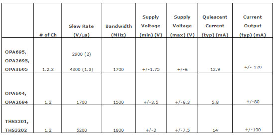
Unlike traditional voltage feedback or fully differential amplifiers, the OPA2695 offers a new level of performance for high-speed applications. Due to its current feedback architecture, the OPA2695 can deliver a high bandwidth of 850 MHz at a gain of +2 V/V and a fast slew rate of 2900 V/µs to process high-speed signals.
The architecture also provides wider bandwidth capability at much higher gains than can be achieved with a voltage feedback architecture. In contrast, fully differential amplifiers, which are popular for differential signal paths and are based on a voltage feedback architecture, suffer from reduced bandwidths at larger gains.
The OPA2695 combines the current-feedback architecture with an optimized differential pin-out, which provides superior gain and bandwidth, maintains high linearity with low harmonic distortion levels, and eases the design process. The pin-out gives super-symmetrical signal paths with input and output pins on opposite sides of the chip to greatly simplify PC board layout.
Supply voltage options increase design flexibility
In addition, designers have the flexibility to provide a single supply voltage (3.5 V to 12 V) or a dual supply voltage (+/-1.75 V to +/-6 V) to the OPA2695 to suit their requirements. For example, with a supply voltage of ±5 V and gain of +8 V/V, the OPA2695 can deliver a large output voltage swing of +/-4.1 V or 8.2 Vpp with a 120 mA sourcing or sinking output drive current into an ADC for accurate digitization.
Alternatively, at a lower single supply voltage of +5 V, the device can save power while still delivering +/-90 mA output current with a 3.4 Vpp for power-sensitive applications, such as handheld portable devices. To further reduce power consumption, a power down option is also available, which reduces the quiescent current consumption to 80 µA.
The OPA2695 extends TI‘s high-speed, current feedback amplifier portfolio, which offers the industry‘s widest bandwidth. [/color][/font]
聲明:本文為中國傳動網(wǎng)獨(dú)家稿件,轉(zhuǎn)載請務(wù)必注明出處。


 網(wǎng)站客服
 粵公網(wǎng)安備 44030402000946號